
TrueInsight
Siemens/Altair Channel Partner
Menu


Simple Wilkinson Power Divider in Altair FEKO
The use of Wilkinson Power Dividers these days is commonplace, but simulating those can be tricky. Check out this Feko Tutorial on how to do that.
Microstrip transmission lines are more cost effective to manufacture than traditional waveguide technology, but that does not mean effective and detailed simulation is unnecessary. Altair FEKO has a wide range of applications, and it just so happens that modeling and simulating microstrips sits comfortably within its suite of features.
Modeling & Simulating a Simple Wilkinson Power Divider in Altair FEKO
To demonstrate just a handful of the capabilities, I’ll be walking through the design and analysis of a simple Wilkinson Power Divider in CADFEKO and POSTFEKO. Fig 1 shows the important parameters chosen for this specific demonstration.
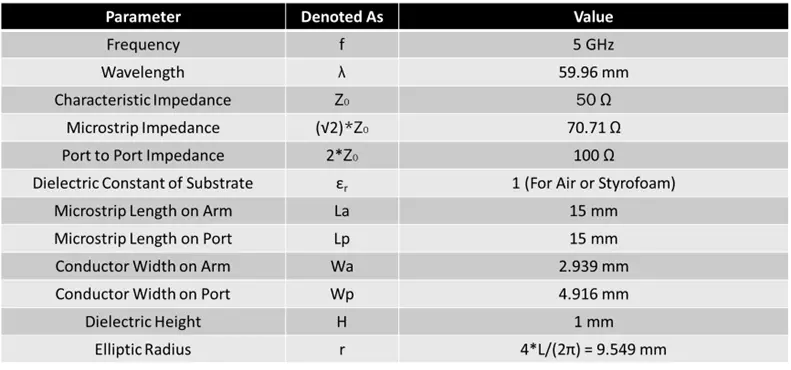 Fig 1. Design Parameters of Wilkinson Power Divider
Our first step is to create the geometry of the conducting material (which we will be using FEKO’s Perfect Electric Conductor or PEC to create) in CADFEKO. To accomplish this, I can construct an elliptic arc with the length and width from the table above. I will use “Path Sweep” to sweep a line equal in length to Wa (2.939 mm) along the length of the arc of length La (15 mm), which will create one of the ‘arms’ of the device. I can them mirror that to create the final shape of the device, excluding the addition of ports. Fig 2, below, briefly depict this process.
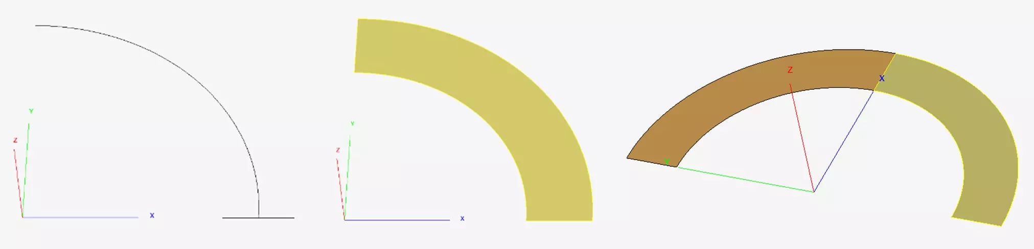 Fig 2: Path Sweep (Left), Arm Creation (Middle), Mirror (Right)
Next, I need to add the ports to the model; ‘port’ here refers to the physical conductor that we will be simulating, but I will discuss the actual ports that tell FEKO how to simulate the model shortly. For this step, I can simply construct a rectangle in the appropriate position, and then copy and transform it to create three ports in total, resulting in Figure 2.
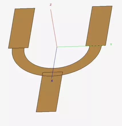 Fig 3: Completed geometry of conductor in device
Next, I’ll need to add space for a dielectric and then the ground plane. Since I am assuming a dielectric with εr equal to 1 (air or Styrofoam), I can just leave a gap equal in depth to the depth of the dielectric between the conductor and ground plane. To make this process easy, I can simply construct a rectangle that covers the surface of the PEC and shift it down by H (1mm in this case), shown in Fig 4.
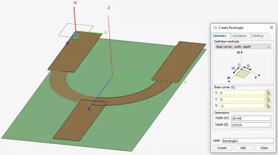 Fig 4: Creating Ground Plane
The final step is to tell the simulation where the ports are, so I’ll create some wires from the physical ports to the ground plane and add the simulated ports to those lines. It is important to note that I also added a line between Ports 2 and 3 in Fig 5, so that I can manually add the impedance of 100Ω between them. Finally, I can make a union from all geometry in the design to tell FEKO they are electrically related, which also meshes the model automatically.
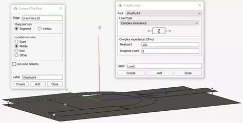 Fig 5: Adding ports to the model.
After setting the simulation request to S-parameters and providing a frequency range, we can run the simulation and move to POSTFEKO. This part of the tool allows us to easily visualize the performance of the device. The first part of our analysis will include a cartesian plot of the S-parameters (in dB) to identify the device’s true operating frequency. Fig 6 shows that the overall best performance occurs at approximately 4.6 GHz.
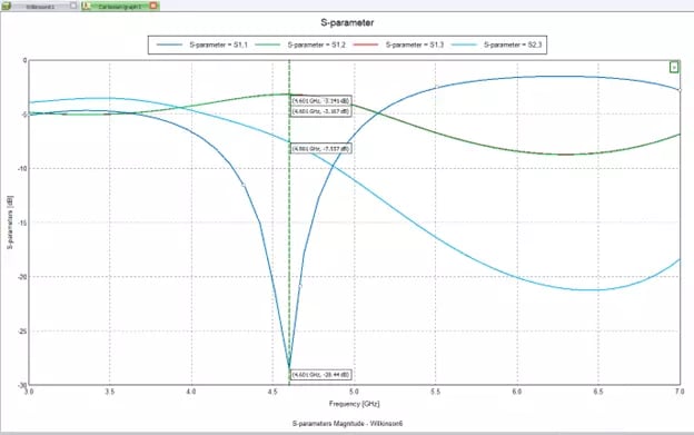 Fig 6: Plot of S-Parameters; Note: S12 and S13 are almost identical and largely overlap.
From this point, we can set up one final analysis, in which we include a near-field request to view the electric field within the device at the newfound operating frequency. To do so, I simply change the frequency to a single value of 4.6 GHz instead of a range of frequencies, create the request by defining a 3D box equal in size and position to the device, click solve once more, and move back to POSTFEKO. I only told FEKO to simulate ten points in the z-direction (‘height’ of the device), but I could have added more or less. Fig 7 shows the resultant electric field at one of the discrete depths in the power divider.
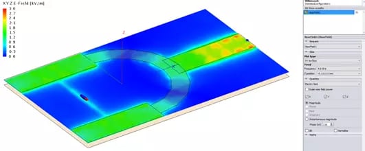 Fig 7: Electric Field within the device from Near-Field Request
Through this blog, we went over the modeling of a Wilkinson power divider and a few forms of analyses in Altair FEKO. I hope this was informative and helpful, but please be sure to reach out if you have any questions about this software specifically or any of our other tools!